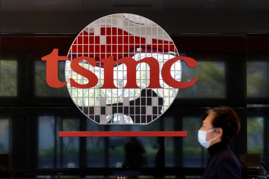
TSMC from Taiwan held more than 70% of the global foundry semiconductor market share in the previous year—10 times higher than Samsung Electronics, which is in second place with about 7%. This is because of the long-standing technological difference in foundry technology between Samsung Electronics and TSMC. Samsung Electronics, whose initial yield for the 3-nanometer, 1 nanometer being one-billionth of a meter, process is still at the 20–30% level, has lost key clients, further increasing the gap with TSMC.
TSMC is striving to take the lead in the worldwide chip manufacturing market through its “super-gap strategy,” moving another step closer to its goal. For this, the company is investing heavily in the upcoming 2-nanometer fabrication process. Che-Chia Wei, TSMC’s chief executive officer, stated on the 15th, “We plan to invest 56 billion dollars, roughly 82 trillion Korean won, in infrastructure this year.” This figure surpasses four times the operating profit of Samsung Electronics from the previous quarter, which was 20 trillion Korean won.
A high-level representative from the semiconductor industry stated, “This is because TSMC’s dominant competitive edge reflects Taiwan’s economic strength, and moreover, the ‘security’ of the nation of Taiwan.”
Samsung Electronics is adopting a position where it will no longer simply observe TSMC’s “superiority.” Drawing on its experience with the 3-nanometer process, it is setting a clear boundary in the 2-nanometer process and quickly improving production efficiency. Specifically, it is demonstrating confidence by continuously implementing the “gate-all-around, GAA, technology,” which it was the first to introduce in the 3-nanometer process, in the 2-nanometer process as well.
GAA is a cutting-edge technology designed to reduce current leakage in semiconductor devices, particularly transistors, in extremely advanced manufacturing processes. Because of this, TSMC has moved away from the older FinFET structure in its 2-nanometer process and instead implemented GAA. Industry experts have noted, “The critical expertise that Samsung Electronics accumulated through experimentation during the 3-nanometer process will serve as a significant advantage for the 2-nanometer process.”
At present, Samsung Electronics is mass-producing the “Exynos 2600,” a crucial chip for Galaxy smartphones, using the first-generation 2-nanometer process, SF2, on the application processor. The product quality is satisfactory, and the initial yield is reported to be higher than anticipated. Samsung Electronics is quickly refining the technology and striving to obtain orders from major tech companies. Tangible outcomes are also being seen. In July of last year, Samsung Electronics obtained an order for Tesla’s AI5·6 chips in the United States. With a value of around 23 trillion South Korean won, it represents the largest single foundry contract in history. It is also reported that discussions are ongoing with Google and AMD regarding the manufacturing of 2-nanometer AI chips. Qualcomm in the United States is also considering the production of next-generation mobile semiconductors using Samsung’s 2-nanometer process.


Leave a comment